High-Performance Micro-LED Platform for AI Innovation
High-Performance Micro-LED Platform for AI Innovation

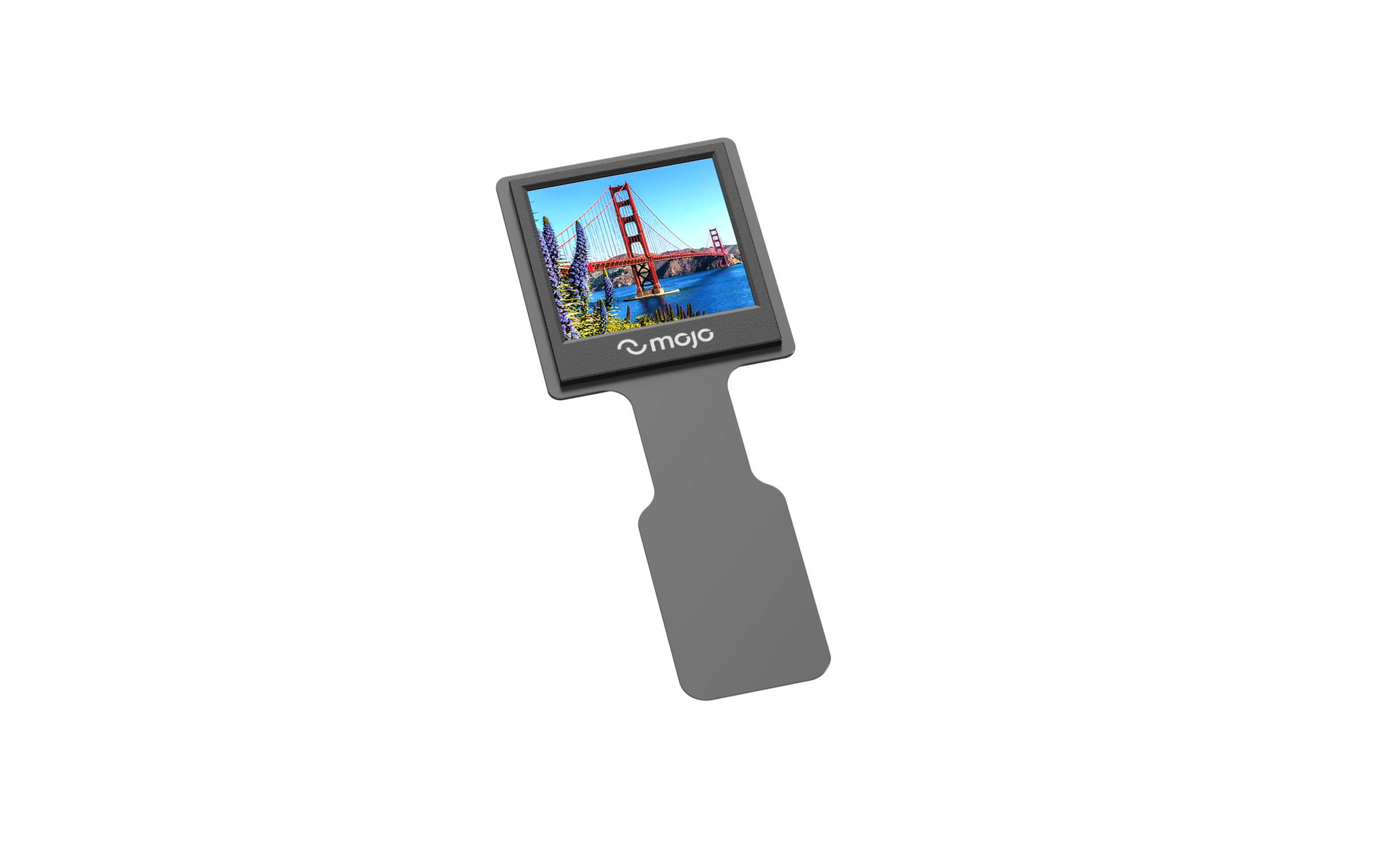
Dynamic Displays for AI Glasses
Mojo’s monolithic RGB micro-LED panel delivers an ultra-compact, high brightness image source with a simplified driving scheme - ideal for next-gen AI Glasses. Our High Performance Quantum Dots (HPQD) enable vibrant color, long-term stability, and high reliability. Our platform is built on three integrated pillars:
Core Technology
- Sub-micron blue micro-LEDs and high-effiency quantum dot ink
Device System
- Optimized CMOS backplane, wafer-to-wafer hybrid bonding, and custom micro-lens optics
Scalable Manufacturing
- 300mm GaN-on-Silicon process for high-volume, cost-effective production
Optical Interconnects for AI Infrastructure
Mojo’s micro-LED platform enables a new class of optical interconnects that meets the power, bandwidth, and reliability demands of large-scale AI systems:
Ultra-Low Power
- Significant reduction in energy per bit
Ultra-High-Density Bandwidth
- Move terabytes of data per mm
CMOS-Ready Integration
- Micro-LEDs are integrated on 300mm wafers and hybrid bonded to any CMOS wafer